

What Happens to a Camera Lens Before It Reaches the Sensor?
Take a photograph.
It feels instantaneous.
Light enters the camera, the sensor captures it, and somehow an image appears on your screen.
Simple, right?
Well, from an optical engineer's perspective, not quite.
Between the real-world scene and the tiny pixels on the image sensor, light has to go through a surprisingly complicated journey. It is refracted, focused, partially reflected, absorbed, distorted, and hopefully—after all that—delivered to the right place with enough contrast to be useful.
That last part is where a good camera lens earns its money.
People sometimes imagine a lens as a piece of glass whose only job is to “focus the image.”
That description is technically true in roughly the same way that saying a Formula 1 car is “a vehicle with four wheels” is true.
There is considerably more going on.
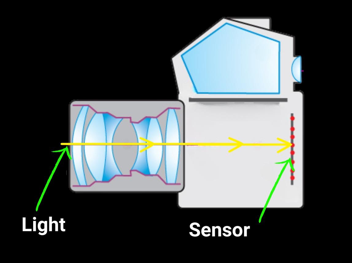
It All Starts With Light From the Scene
Before the lens does anything, there is the scene itself.
Every object in front of the camera reflects or emits light. That light travels toward the camera from different directions and with different wavelengths.
A red car, for example, does not simply send “red light” toward the camera in one neat beam. Light arrives from different parts of the vehicle, at different angles, with different intensities.
The lens has to take this chaotic collection of light rays and organize it into an image.
That's essentially the optical system's job:
Take light coming from different directions and make it form a controlled image on the sensor.
And immediately, there is a problem.
Light does not naturally behave the way engineers would like it to.
When light passes from air into glass, its direction changes. When it passes through another optical element, it changes again.
This is called refraction.
By carefully selecting the shape and material of each optical element, lens designers use this behavior to control where the rays eventually meet.
That is why a camera lens can contain several optical elements rather than one simple piece of glass.
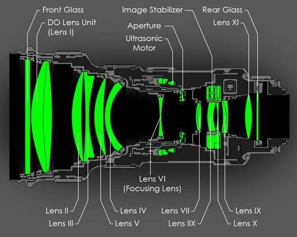
The Lens Is Not One Lens
Look at a modern camera lens and you may see a small cylindrical object.
Inside, however, there can be multiple optical elements.
Each element has a job.
Some help focus the image. Others correct aberrations. Some improve edge performance. Some help control distortion or chromatic aberration.
The interesting part is that these elements do not work independently.
They work as a system.
A designer might change the curvature of one element and then need to adjust another element to compensate for the effect.
Change the aperture and the optical behavior can change again.
Make the lens smaller and the design becomes more difficult.
Increase the field of view and distortion becomes harder to control.
Demand F1.0 performance and the optical designer gets another headache for free.
This is why optical design is fundamentally an exercise in compromise.
You rarely get to maximize everything simultaneously.
Then Comes the Aperture
Somewhere inside the optical system is the aperture.
You can think of the aperture as the “gatekeeper” controlling how much light enters the lens.
An F1.0 lens has a very large relative aperture, allowing significantly more light into the optical system than a smaller-aperture lens.
This becomes especially important in low-light imaging.
But there is a catch.
A larger aperture does not simply mean “better.”
When you open up the aperture, more rays from the outer portions of the optical system are involved in forming the image. These rays are generally harder to control.
As a result, aberrations can become more noticeable.
This is one reason designing a high-performance F1.0 lens is much more challenging than simply making the aperture physically larger.
For applications such as night surveillance, however, the trade-off can be worthwhile.
When the available light is limited, collecting more of it can make the difference between a useful image and a noisy one.
Not Every Ray Arrives at the Sensor the Same Way
Here's a detail that becomes particularly important when selecting a lens for a modern image sensor:
The angle at which light reaches the sensor matters.
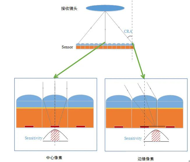
Engineers often talk about the Chief Ray Angle, or CRA.
In simple terms, CRA describes the angle of the chief ray reaching different areas of the sensor.
Why should we care?
Because modern image sensors are not simply flat pieces of light-sensitive material waiting patiently for anything to hit them.
There are microscopic structures above the photodiodes, including microlenses and other layers.
If incoming light arrives at an unsuitable angle, especially toward the edge of the sensor, the sensor may not use that light as efficiently as expected.
This is one reason lens and sensor matching matters.
A lens can have the correct focal length and sensor format and still not be an ideal optical match.
The Image Circle: Will the Lens Actually Cover the Sensor?
Here's another surprisingly common issue.
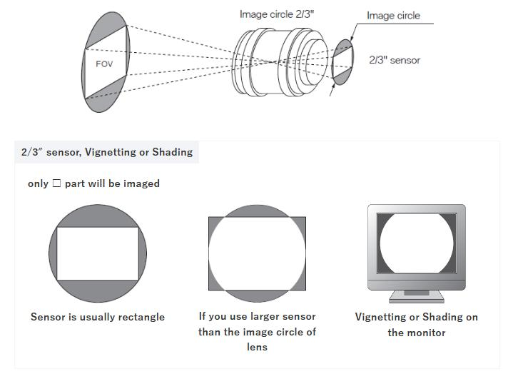
A lens produces an image circle.
The sensor sits inside that image circle and uses the portion that falls on its active area.
If the image circle is too small, the corners of the sensor may not receive sufficient image information.
The result can be vignetting or even visible dark corners.
This is why sensor format matters.
A lens designed for a smaller sensor cannot simply be attached to a much larger sensor and expected to perform perfectly.
You might physically connect the two.
Optically, however, the relationship may be rather less cooperative.
This is also why engineers look at the actual sensor dimensions rather than relying only on labels such as “1/2.7-inch” or “1/1.8-inch.”
Those format names are useful shorthand, but the actual active area and optical requirements are what ultimately matter.
And Then There Are Aberrations
Here is where optical engineering becomes a little less glamorous.
Light passing through a real lens does not always focus exactly where we want it to.
Different wavelengths can behave differently.
Rays passing through different parts of a lens may also focus differently.
This creates various optical aberrations.
Chromatic aberration can produce color fringing.
Spherical aberration can reduce image sharpness.
Astigmatism can affect how fine details are reproduced.
Coma can make point-like objects appear distorted, especially toward the edges.
And field curvature means that the plane of best focus may not behave like the perfectly flat sensor engineers would prefer.
None of these problems sound particularly exciting.
But they are exactly the sort of things that determine whether a lens produces a crisp image or something that looks suspiciously like it needs glasses.
Modern optical design is largely about controlling these imperfections.
The Image Is Not Equally Sharp Everywhere
This brings us to one of the biggest misunderstandings about lens resolution.
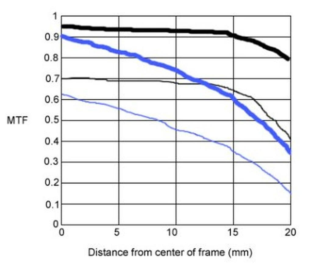
A lens does not necessarily perform equally well at the center and at the edge.
The center of the image is usually easier to control.
As you move toward the edge, optical performance can decline.
This is particularly important for wide-angle lenses.
Imagine a surveillance camera monitoring a parking lot.
The center of the image may be extremely sharp.
But what happens when a vehicle enters from the side?
If edge resolution is poor, the camera may technically have a high-resolution sensor while delivering much less useful detail where it matters.
This is why optical engineers look at MTF performance across the image field, rather than simply asking whether a lens is “4MP” or “8MP.”
The number of pixels tells you what the sensor can sample.
MTF helps tell you how effectively the optical system can deliver detail to those pixels.
Before the Light Finally Reaches the Sensor
Even after passing through the lens elements, aperture, and optical corrections, the light may encounter additional components.
Depending on the camera design, the optical path can include:
Protective windows
IR-cut filters
Sensor cover glass
Low-pass filters
Other optical coatings or structures
Each additional surface can influence the optical system.
Reflection can reduce transmission.
Poor coatings can increase flare or ghosting.
The thickness and refractive properties of components in front of the sensor can also affect focus and optical performance.
This is particularly important in compact camera systems where everything is packed into a very small space.
The optical designer cannot simply say:
“That's the sensor manufacturer's problem.”
The entire optical stack matters.
Finally, the Light Reaches the Sensor
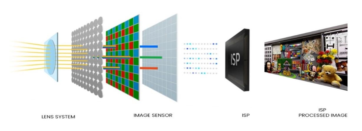
After all these interactions, the light finally reaches the image sensor.
The sensor converts incoming photons into electrical signals.
At this point, it may seem that the lens has finished its job.
Actually, this is where you can finally see whether the lens did its job well.
If the optical system delivered:
Enough light
Good contrast
Fine detail
Controlled aberrations
Appropriate ray angles
Adequate image coverage
the sensor has useful information to work with.
If not, the image-processing system has a difficult problem on its hands.
Noise reduction can reduce noise.
Sharpening can enhance edges.
AI algorithms can improve images.
But software cannot perfectly recover optical information that was never captured.
That is why optical quality remains important even as computational imaging becomes more sophisticated.
Why Lens and Sensor Selection Should Happen Together
This is probably the practical lesson I would emphasize most strongly.
Don't choose a sensor first and then casually ask:
“Which lens can we put on it?”
For many projects, lens and sensor selection should be considered together.
The engineer needs to understand the relationship between:
Sensor + Lens + Aperture + Field of View + Image Processing + Lighting
A change to one part can affect the others.
A smaller pixel size can increase optical resolution requirements.
A wider field of view can increase distortion and edge-performance challenges.
A larger aperture can improve low-light performance while making aberration control more difficult.
A different sensor can change CRA requirements.
This is why experienced optical suppliers often ask surprisingly detailed questions before recommending a lens.
It is not because they enjoy paperwork.
Usually, they are trying to avoid recommending something that looks perfect on paper and disappoints you when connected to the actual camera.
The Optical Path Is Really a Chain of Decisions
Once you understand what happens between the scene and the sensor, one thing becomes clear:
A camera lens is not simply “focusing light.”
It is managing light.
Every optical surface, every curvature, every spacing, every coating, and every mechanical tolerance affects the final image.
The lens has to collect enough light.
It has to direct that light correctly.
It has to control aberrations.
It has to provide sufficient resolution.
It has to match the sensor.
And ideally, it needs to do all of this thousands or millions of times with consistent performance.
That is why a small camera lens can contain an impressive amount of engineering.
At Boshi Optics, optical solutions are developed for applications ranging from security surveillance and AI vision to drones, automotive imaging, medical devices, and other imaging systems. The company's manufacturing capabilities cover optical component processing, precision molding, injection molding, lens assembly, and optical testing.
The final image may look simple.
The journey that created it is anything but.
One Last Way to Think About It
The next time you look at a camera specification and see:
8MP Sensor
don't immediately imagine eight million tiny pieces of detail.
Imagine eight million opportunities to record information.
Then ask:
What did the lens actually deliver to them?
That question is much closer to the heart of optical engineering.
Because the sensor records the image.
But before the sensor can record anything, the lens has to give it something worth recording.